Mouse Adventures #6: Enabling the Bootloader
Wherein I explore various different methods to try and get my mouse into bootloader mode so I can flash it. It didn't get me anywhere, but it's all about the journey, right?
The Previous Five Parts
Back in Part 1, I started this trip with an introduction to the mouse and the mechanism used by the config tool to retrieve notifications from it (good old HID Report ID 6). In Part 2 and Part 3, I extracted and disassembled the firmware, and in Part 4, I started sending my own commands to the mouse... only to be cut short when the config tool bricked it while I was trying to figure out the format for button mappings. Finally, in Part 5, I began trying to make sense of the disassembly so I could learn more about what was going on.
We're at a bit of an impasse now. It would be really good to get this thing back into a working state so that we can start sending it commands again. It's got a firmware update mechanism, and we've got tools for that, as well as the firmware file itself. We can't quite rely on the mouse's supplied updater though, as it uses the 0xA and 0x8A commands to switch the mouse into bootloader mode, and that's not working. Is there another way to do that? To the Holtek HT68FB5x0 datasheet!
Searching the Datasheet
Page 27 describes "In System Programming", saying that the flash can be programmed through the USB interface. "The technical details regarding the in-system programming of the devices are beyond the scope of this document and will be supplied in supplementary literature." Of course... that would be too convenient.
Page 29 describes the ISP bootloader. It says that the Holtek bootloader occupies 0.5K words in the Flash memory, meaning that the accessible portions of the flash are 0000h to 3DFFh. No further information.
Page 33 describes "In Application Programming", which is how the device makes changes to its own flash. There's a description about how to enable writing and write to the flash through an intricate series of register writes and magical incantations. Ultimately, this isn't of much use to us at this point - if we could write new code to the chip right now, we wouldn't be searching for one of these methods!
Page 37 describes "In Circuit Programming", saying that the flash can be programmed using a 4-pin interface. "The technical details regarding the in-circuit programming of the devices are beyond the scope of this document and will be supplied in supplementary literature." Again.
They give us details about the electrical connections required for this last scheme: you have to connect the chip's UDN pin to a writer's ICPDA pin (for 'programming serial data'), the chip's RES pin to a writer's ICPCK pin ('programming clock'), and the VDD and VSS pins for power supply and ground respectively. It's something, but we don't have enough information to be able to usefully take advantage of this.
Searching the Application Notes
There's a lot of Application Notes on the Holtek website which describe how to accomplish a wide variety of things. We're interested in the ones within the '8-Bit Flash MCU' section. There's some stuff that seems relevant to our chip, and elaborates on details not covered in the datasheet.
HT8 MCU IAP Application Guidelines: More about writing to the chip from code running on the chip. Potentially useful later, but not just now.
HT8 MCU ICP Application Guidelines: Explains how to design a circuit board in order to allow reliable in-circuit programming (writing to the chip while it's installed into a device). Nifty, but this requires me to have a Holtek programmer (an e-Writer Pro or e-Link). I don't have one of these.
HT8 MCU ISP Application: Finally, a description of how the bootloader works!
Both the HT66FB5x0 and HT68FB5x0 series of devices support a Bootloader function, which can be used to update the Flash program memory using the ISP function. The Bootloader Code will be executed if the library or a subprogram is called to enable the Bootloader Code after a reset or power-on reset when the MCU is executing user code. At this time, new programs can be loaded from a PC via a USB interface to update the Flash memory program and then be executed after the MCU is re-powered on with corresponding configurations.
Encouraging. According to this, you can select what kind of bootloader to use when you're building your project in HT-IDE3000.
There's a flowchart, a guide and some example C code for this. It's actually quite straightforward: Holtek gives you a library called Enable_Bootloader.lib containing the ~magic code~ to enable the bootloader. You call a function from that library, and if a global flag has been set, then you can reboot the controller (either by unplugging the device and plugging it back in, or by triggering a 'Watchdog Timer Overflow'), and it should enter bootloader mode.
Presumably this is what happens when you send the mouse the magic 0xA/0x8A commands. It sheds a bit of light on what's probably going on behind the scenes, but it doesn't directly help us.
Enabling the Bootloader (MCU-Side)
I dug through the disassembly to see if I could figure out what was going on. When I'd previously tried to gather some info from it, I was able to name some code addresses and global variables by comparing similar/identical code blocks between my mouse's firmware and the Holtek sample code. I was able to find the code that handles command 0xA, and subsequently the code that enables the bootloader, which is as follows (I've removed unrelated code from this sample for brevity's sake):
FeatureCommand0A_071Ch:
; verify that all the parameters match the expected values by setting
; USB_Temp2 to (out2 ^ 0xAA) | (out3 ^ 0x55) | (out4 ^ 0xCC) | ...
071c : 0faa : mov a, AAh
071d : 4462 : xor a, FIFO_Request   ;out2
071e : 40df : mov USB_Temp2, a
071f : 0f55 : mov a, 55h
0720 : 4463 : xor a, FIFO_wValueL   ;out3
0721 : 45df : orm a, USB_Temp2
0722 : 0fcc : mov a, CCh
0723 : 4464 : xor a, FIFO_wValueH   ;out4
0724 : 45df : orm a, USB_Temp2
0725 : 0f33 : mov a, 33h
0726 : 4465 : xor a, FIFO_wIndexL   ;out5
0727 : 45df : orm a, USB_Temp2
0728 : 0fbb : mov a, BBh
0729 : 4466 : xor a, FIFO_wIndexH   ;out6
072a : 45df : orm a, USB_Temp2
072b : 0f99 : mov a, 99h
072c : 4467 : xor a, FIFO_wLengthL  ;out7
072d : 45df : orm a, USB_Temp2
; if all of those had the correct values, then USB_Temp2 should now be zero
072e : 50df : sz USB_Temp2
072f : 2e95 : jmp ClearCmdIndex_0695h
; ...and if that was theh case, we can make this call
0730 : 67bc : call SwitchToBootloaderMode_0FBCh
0731 : 2e95 : jmp ClearCmdIndex_0695h

; flash registers by bank/offset
; (registers in bank 1 require indirect reads/writes using BP, MP1, IAR1)
;        1:40h : FRCR : control (flags FSWRST, CLWB)
;        1:41h : FCR  : control (flags CFWEN, FMOD2-0, BWT, FWT, FRDEN, FRD)
; 0:42h, 1:42h : FARL / FARH : address
; 0:43h, 1:43h : FD0L / FD0H : read/write data 0
; 0:44h, 1:44h : FD1L / FD1H : read/write data 1
; 0:45h, 1:45h : FD2L / FD2H : read/write data 2
; 0:46h, 1:46h : FD3L / FD3H : read/write data 3

SwitchToBootloaderMode_0FBCh:
0fbc : 3410 : clr EMI      ; disable interrupts
0fbd : 0f01 : mov a, 01h
0fbe : 0084 : mov BP, a    ; access bank 1 for the flash registers
0fbf : 0f41 : mov a, offset FCR
0fc0 : 0083 : mov MP1, a   ; IAR1 now points to FCR

; clear the flag in preparation to call WriteMagicFlashSequence
0fc1 : 7791 : clr [91h].7

; write 0xE8 to FCR: 1110 1000 (see datasheet page 32)
;   CFWEN = 1   (Flash ROM Write Enable bit)
;   FMOD  = 110 (Flash Memory Write Enable bit control mode)
;   BWT   = 1   (activate a mode change cycle)
;   FWT   = 0   (no writing is occurring right now)
;   FRDEN = 0   (reading is disabled right now)
;   FRD   = 0   (no reading is occurring right now)
0fc2 : 0fe8 : mov a, E8h
0fc3 : 0082 : mov IAR1, a

; send the sequence to enable flash writing
0fc4 : 67f2 : call WriteMagicFlashSequence_0FF2h

; set the flag that triggers the alternate sequence
0fc5 : 7391 : set [91h].7

; write 0xF8 to FCR: 1111 1000
;  all properties the same as before, but FMOD is now 111
;  the datasheet says this is 'reserved'
0fc6 : 0ff8 : mov a, F8h
0fc7 : 0082 : mov IAR1, a

; send the sequence to enable... /something/?
0fc8 : 67f2 : call WriteMagicFlashSequence_0FF2h

; write 0xD8 to FCR: 1101 1000
;  FMOD is now 101: another 'reserved' mode!
0fc9 : 0fd8 : mov a, D8h
0fca : 0082 : mov IAR1, a  ; write D8 to FCR

; we're gonna send that sequence again, for some reason
0fcb : 67f2 : call WriteMagicFlashSequence_0FF2h

0fcc : 0f1f : mov a, 1Fh
0fcd : 0087 : mov TBLP, a
0fce : 1f09 : clr TBHP     ; set the table registers to 001F

; write 0x90 to FCR: 1001 0000
;  FMOD is now 001: page erase mode
;  BWT is now 0: no mode change requested (weird but ok)
; also write address from TBHP/TBLP into FARH/FARL: 001F
0fcf : 0f90 : mov a, 90h
0fd0 : a026 : call SetFlashModeAndAddressRegisters_1026h

; activate a write cycle and wait for it to finish
0fd1 : a047 : call ActiveFlashWriteCycle_1047h

; write 0x80 to FCR: 1000 0000
;  FMOD is now 000: write memory mode
; also write address: 001F
; we haven't changed TBHP/TBLP since, so this remains the same
0fd2 : 0f80 : mov a, 80h   ; Write mode
0fd3 : a026 : call SetFlashModeAndAddressRegisters_1026h

; writing 5A64 to 001F
0fd4 : 0f43 : mov a, offset FD0H
0fd5 : 0083 : mov MP1, a   ; data addr
0fd6 : 0f64 : mov a, 64h
0fd7 : 00c3 : mov FD0L, a  ; datalow:  64
0fd8 : 0f5a : mov a, 5Ah
0fd9 : 0082 : mov IAR1, a  ; datahigh: 5A

; activate a write cycle and wait for it to finish
0fda : a047 : call ActiveFlashWriteCycle_1047h

; now IAR1 points to FCR again
; write 0xB2 to FCR: 1011 0010
;  FMOD is now 011: read memory mode
;  FRDEN is now 1: enables reading of flash memory
0fdb : 0fb2 : mov a, B2h
0fdc : a026 : call SetFlashModeAndAddressRegisters_1026h
0fdd : 1583 : dec MP1     ; point to FCR again so we can manipulate it it
0fde : 3002 : set IAR1.0  ; set FCR.FRD: activate read cycle

; wait for the read cycle to finish
0fdf : 0001 : clr wdt
0fe0 : 3c02 : sz IAR1.0   ; if FCR.FRD is 1,
0fe1 : 6fdf : jmp $-2     ; then jump back to 0FDFh

; clear some global flag
0fe2 : 7511 : clr [91h].2

0fe3 : 0743 : mov a, FD0L ; read byte
0fe4 : 0c64 : xor a, 64h  ; we expect it to be 64
0fe5 : 3d0a : sz Z        ; if (byte_that_was_read ^ 0x64) == 0...
0fe6 : 7111 : set [91h].2 ; then set that global flag

0fe7 : 3782 : clr IAR1.7  ; disable FWEN (write enable)
0fe8 : 3010 : set EMI     ; re-enable interrupts
0fe9 : 0003 : ret

WriteMagicFlashSequence_0FF2h:
; write 0400 to FD1H and FD1L
0ff2 : 0f44 : mov a, offset FD1H
0ff3 : 0083 : mov MP1, a
0ff4 : 0f00 : mov a, 00h
0ff5 : 00c4 : mov FD1L, a  ; write 00 low
0ff6 : 0f04 : mov a, 04h
0ff7 : 0082 : mov IAR1, a  ; write 04 high

0ff8 : 1483 : inc MP1      ; MP1 now points to FD2H

; write 090D to FD2H and FD2L
0ff9 : 0f0d : mov a, 0Dh
0ffa : 00c5 : mov FD2L, a  ; write 0D low
0ffb : 0f09 : mov a, 09h
0ffc : 0082 : mov IAR1, a  ; write 09 high

0ffd : 1483 : inc MP1      ; MP1 now points to FD3H

; write 40C3 (flash enable) or 2035 (bootloader enable)
; depending on the value of the flag at [91h].7
0ffe : 0fc3 : mov a, C3h   ; if flag 0, then do C3h low
0fff : 7f91 : sz [91h].7
1000 : 0f35 : mov a, 35h   ; if flag 1, then do 35h low
1001 : 00c6 : mov FD3L, a
1002 : 0f40 : mov a, 40h   ; if flag 0, then do 40h low
1003 : 7f91 : sz [91h].7
1004 : 0f20 : mov a, 20h   ; if flag 1, then do 20h high
1005 : 0082 : mov IAR1, a

; wait for the mode change to complete
1006 : 0f41 : mov a, offset FCR
1007 : 0083 : mov MP1, a   ; FCR offset
1008 : 0001 : clr wdt
1009 : 3d82 : sz IAR1.3    ; is FCR.BWT clear?
100a : a808 : jmp $-2      ; if BWT is 1, loop back around

; "FWEN: Flash ROM Write Enable bit"
; 0: disabled; 1: unimplemented
;
; datasheet, page 32: it's ineffective to set this bit to high
; Holtek engineers: HOW ABOUT I DO ANYWAY
100b : 3382 : set IAR1.7   ; set FWEN
100c : 0003 : ret

SetFlashModeAndAddressRegisters_1026h:
; we assume at this point that IAR1 points to FCR, i.e. MP1 is 41h
1026 : 0082 : mov IAR1, a
1027 : 1483 : inc MP1       ; given that assumption, IAR1 should now point to FARH
1028 : 0707 : mov a, TBLP
1029 : 00c2 : mov FARL, a
102a : 0709 : mov a, TBHP
102b : 0082 : mov IAR1, a
102c : 0003 : ret

ActiveFlashWriteCycle_1047h:
1047 : 0f41 : mov a, offset FCR
1048 : 0083 : mov MP1, a
1049 : 3102 : set IAR1.2   ; set FWT to activate a write cycle

; wait for FWT to become 0 (signifying that the write cycle has finished)
104a : 0001 : clr wdt
104b : 3d02 : sz IAR1.2    ; if FWT is still set, repeat
104c : a84a : jmp $-2
104d : 0003 : ret
There's a lot going on here, no getting round it. Rather than trying to explain each bit after-the-fact as usual, I've just added a lot of inline comments into the disassembly. Let's go over the SwitchToBootloaderMode function. As it turns out, the HT8 MCU IAP Application Guidelines are helpful here...
The first part of that document explains how to enable writing to flash memory. You must select a specific mode using the FMOD field in FCR (the Flash Control register) and set the Write Enable control bit. Then, you get 300 microseconds to write a magic sequence into data registers 1, 2 and 3: 0400, 090D and 40C3.
The bootloader enable function does this, using a helper function I've called WriteMagicFlashSequence. Then, it goes completely off the rails into undocumented territory: it sets FMOD to 111 ('reserved' according to the datasheet), writes the magic sequence 0400 090D 2035, sets FMOD to 101 (also 'reserved'!) and writes the magic sequence 0400 090D 2035 again.
Following that mess, it begins what looks like a normal write process in accordance with the IAP guidelines. It's writing to address 001F. It enables page erase mode, performs a write cycle, enables write mode, writes the word 5A64 and performs another write cycle.
Then, it enables read mode and reads back from address 001F. It performs a read cycle and clears a global flag. It reads a low byte, and if that byte is 0x64, it sets that global flag. Finally, no matter what the result of that was, it disables FWEN (the write enable mode), re-enables interrupts, and finishes its work.
So... does this help us? There's some secret, undocumented stuff going on here: this is all part of Holtek code which they distribute simply as a library for device developers to link into their MCU code.
Part of this code looks like a normal write sequence. The word 0x5A64 is written to address 001F, and then it's read back, and the low byte is checked to see if it was written successfully. However, for all we know, this might be doing something else that isn't a write at all. We're in undocumented territory here, after all - the datasheet's implied contract for how the flash memory operates stopped having a single iota of meaning as soon as this function put the flash memory into a 'reserved' mode.
It's pretty interesting, but it's not going to get us anywhere in this situation where we can't actually write any code to the device. Back to the drawing board we go.
Enabling it through hardware... maybe?
If there's a bootloader running before the mouse's firmware, there's a chance that there might be a way to force it into the ISP mode so that we can re-flash it. This MCU has a lot of pins, perhaps there's something we can short during the boot process. It's worth a look, at least. Time to tear down this mouse.
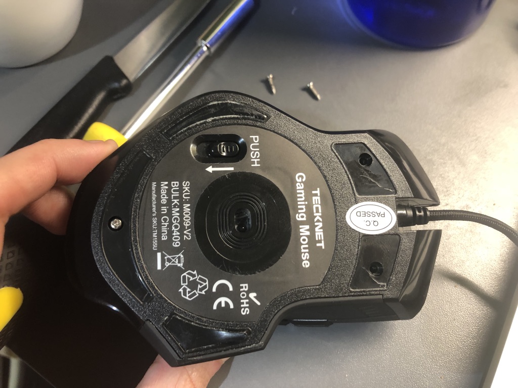
First, it's probably a good idea to take out the compartment containing the metal weights. You can use a knife to gently prise off the two glued-on feet adjacent to the cable and the one at the bottom of the mouse. Each one conceals a screw.

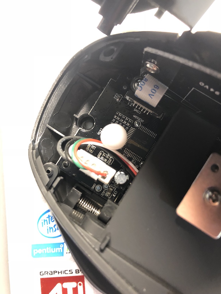
You can then lift the top half of the casing off. There's a small circuit board on that half for the DPI +/- buttons, connected to the rest of the mouse using three wires fed into a connector. Carefully detach the connector and the top half will come off, granting you a better view. There's that Holtek-branded chip, in its square 48-pin package.
You can see a big point marked 'OCDSDA' next to the corner. If we believe that label, then it's presumably connected to the PA0/TCK1/OCDSDA pin on the MCU. The datasheet informs us that this is "general purpose I/O" (in its PA0 form), "TM1 input" (in its TCK1 form) and "Debug Data I/O" (in its OCDSDA form). The latter is only relevant for debugging variants of the MCUs (HT68VB560), though - we've got a production MCU, HT68FB560.
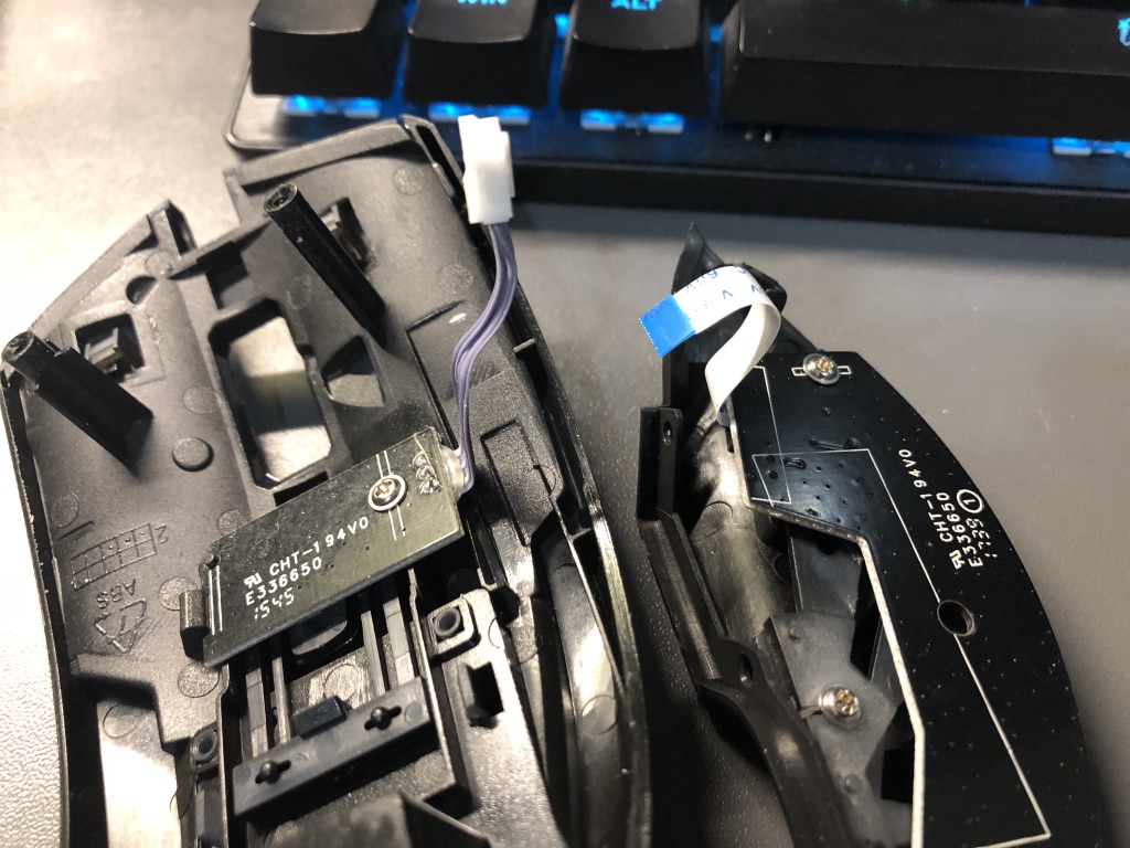
Next up, let's free the side buttons. There's a tiny connector with a blue ribbon cable right behind the OCDSDA point. Lift up the bit on top that retains it and you'll be able to gently remove the cable, allowing you to lift the side assembly free.
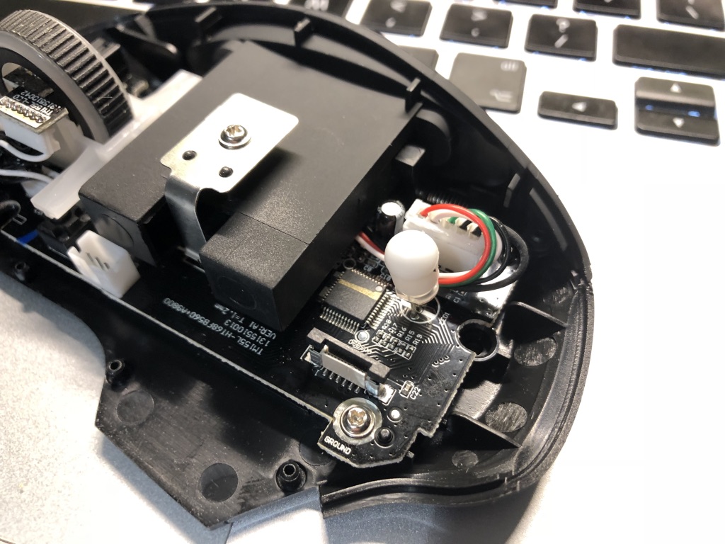
To access the middle portion of the board, you'll need to first unscrew and detach the metal bracket covering the rectangular container that holds the weight tray. Alas, that's not quite enough to release it - there's a tiny black screw hidden on the mouse's underside, behind the rest closest to the slot. Once you've unscrewed that and removed the bracket, you can detach the compartment - albeit you may need to fiddle a bit with the spring-loaded catch in order to work it free.
Astute observation there, Windows 10!
We can now see the Avago A9800 sensor, connected to the MCU via traces on the board. We can see another point on the opposite corner of the MCU which was previously covered up by the compartment: 'RESET'. I played around with this a bit. Shorting the RESET pin to ground resets the mouse (as you might expect!), but doesn't do anything interesting - it just goes straight back into its regular mode.
At this point I didn't know what else to try - I was nervous as I didn't want to risk damaging the hardware - so I decided to go back to the software side of things. Barring some major discovery on the bootloader side of things, or me blowing 60€ plus tax plus shipping on an e-Writer Pro, it looks like my only hope is going to be finding something in the firmware that will allow me to activate the bootloader mode.
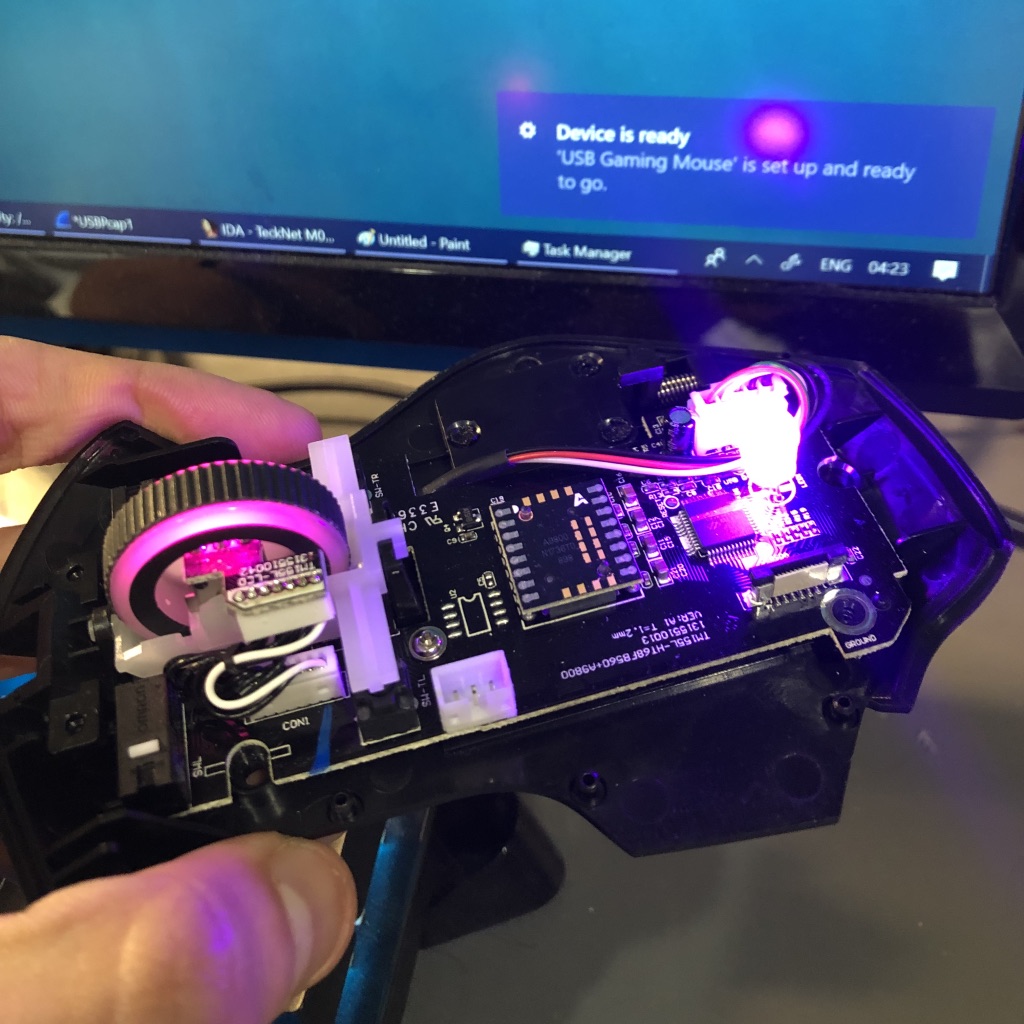
It appears to be pretty shoddily programmed (which is how I got myself into this mess in the first place). The mouse is still working to an extent: it turns on its lights, it successfully associates to my computer, it delivers USB descriptors, I can click, I can use the wheel (kind of). Maybe I can figure out why it's stopped responding to commands. If I can manage that, then perhaps I can figure out a way round that.
I'm going to need better analysis tools, though.
Coming Soon
In Part 7 I'll write an IDA processor module so that we can more effectively figure out what's going on in the mouse's firmware. There's only so long I can spend doing careful find-and-replace every time I want to rename a memory location after I figure out a possible use for it.
If you've really enjoyed this series of posts and want to help fund my hot chocolate habit, feel free to send me a couple of pounds: Ko-fi | Monzo.me (UK) | PayPal.me
Previous Post: Mouse Adventures #5: Dumping and Parsing the USB Descriptors
Next Post: Mouse Adventures #7: Writing an IDA Processor Module